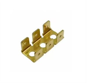
The high-precision stamping used for switches has a series of unique characteristics and advantages.
Firstly, it can ensure that the size and shape of switch components meet extremely high precision requirements. This means that key components such as the contact points and shrapnel of the switch can be accurately matched, ensuring the accuracy and reliability of switch operation. For example, in microswitches, high-precision stamped contacts can achieve extremely sensitive and stable contact.
Secondly, this process can produce switch components with complex shapes and fine structures. For example, the complex terminal structures of some multipole switches can be formed in one go through high-precision stamping, reducing subsequent processing steps.
Furthermore, high-precision stamping can ensure the smooth and even surface quality of switch components, reduce friction and wear, and extend the service life of switches.
In addition, it also has efficient production characteristics and can produce high-quality switch stamping parts on a large scale in a short period of time, meeting the large demand of the market.
In practical applications, high-precision stamping parts used for mobile phone button switches can provide comfortable pressing sensation and accurate response; In the field of industrial control, high-precision stamping ensures the stable performance of switches in harsh environments.
High precision stamping is widely used in the field of electronic products. This technology can meet the demand for high-precision and high-quality components in electronic products, providing strong support for the development of the electronic product industry.
Firstly, high-precision stamping is widely used in the manufacturing of electronic product casings such as mobile phones and tablets. These casings typically require a certain level of strength and exquisite appearance, and high-precision stamping technology can ensure the accuracy and quality of the casings while improving production efficiency. Through precise mold design and stamping processes, electronic product casings with complex shapes and precise dimensions can be manufactured to meet the aesthetic and usage needs of consumers.
Secondly, high-precision stamping is also used to manufacture internal components of electronic products. For example, key components such as electronic connectors and connectors have extremely high requirements for accuracy and reliability. High precision stamping technology can ensure the dimensional accuracy and shape consistency of these components, and improve the overall performance and stability of electronic products.
In addition, high-precision stamping is also applied in the manufacturing of electronic components, such as lead frames and shielding covers for integrated circuits. These parts need to have characteristics such as high precision, small shape, and thin material to meet the manufacturing requirements of integrated circuits. High precision stamping technology can achieve high-speed and precise stamping processing, ensuring the quality and performance of the lead frame.
With the continuous development of the electronic product market and technological progress, the application prospects of high-precision stamping in the field of electronic products will be even broader. In the future, high-precision stamping technology will continue to improve, providing more high-quality and high-precision components for the electronic product industry, and promoting the sustainable development of the entire industry.